
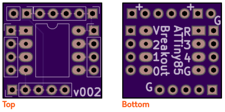
ATTiny Breakout v002 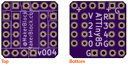
ATTiny Breakout v004
It is pretty incredible that you can find a written or1 video tutorial on virtually any topic to learn anything. Today, I’m particularly thankful to Shawn Hymel, Sparkfun, and Digi-Key for putting together their Intro to KiCAD video series on printed circuit board design.
This series took me from knowing nothing at all about PCB layout and design to ordering my very first board through OSHPark. My first design isn’t anything amazing – it was basically a breakout board for an ATTiny85 to make it easier to build small projects.
My first ATTiny hacked tap light was a mess. I soldered wires directly to the microcontroller making it a real pain to update. ((I ask you – is this the work of a sane man?)) I soon realized my mistake and soldered an 8-pin socket in its place so I could reprogram the chip easily.
Mercifully, Shawn’s tutorial series got me up and running very quickly. This post is not meant to be a tutorial for KiCAD, but more like a “lab notebook” for the workflow to create a board. If you haven’t built a board yet, go check out Shawn’s series and follow along in KiCAD. If you are a novice like me, you might find these notes helpful:
Eeschema
- If you launch Eeschema separately from KiCAD, you can save different versions of a schematic. Keeping old versions of design files is hugely helpful to me and if you launch KiCAD directly, the option to save different file names and versions is not available!
- The keyboard shortcuts in Eeschema are great. With just a few, it’s possible to really get around quickly.
- “Shift-A” and left click to place parts
- “M” to move parts
- “R” to rotate parts
- It is necessary to add “PWR_FLAG” to both the power and ground lines.
- Double check your connections work by clicking on the bug icon.
- Assign the parts you intend to use to match up with the symbols using the “Assign PCB footprints” icon.
- Save your work and “Generate netlist” to have something the Pcbnew will be able to work with.
Pcbnew
- First configure the Design Rules by going to Setup -> Design Rules. Shawn pulled these KiCAD Design Rules from the OSHPark.com website. KiCAD has apparently changed a little since the version used on the OSHPark website, but the settings are easy enough to identify and change.
- Net Classes Editor
- Clearance: 0.01. Track Width: 0.01. Via Dia: 0.03. Via Drill: 0.015. uVia Dia: 0.03. uVia Drill: 0.015. Diff Pair Width: default. Diff Pair Gap: default.
- Minimum track width: 0.006. Minimum via diameter: 0.027. Minimum via drill: 0.013Custom Track Widths: Track 1: 0.03
- Net Classes Editor
- Read netlist” to bring your design over from Eeschema.
- Placing parts and drawing lines gets a lot easier when you fine tune the Grid. I started with 5.00 mils at first, then smaller figures to place smaller parts and features.
- Once the parts are arranged in Pcbnew, connect the ground and power lines using 30 mil traces and everything else using 10 mil traces.
- Create the outline for the board cutout by clicking on “Edge.Cuts” and drawing with the “Add graphic lines” tool. Starting with my second board, I began cutting the corners off, so that they were a little nicer to hold and
- Label things on the “F.SilkS” and “B.SilkS” layers using the “Add text”‘ button. Since my boards are so small, I wanted the text to be a fair bit smaller than the default settings. I edited the text settings by going to Setup -> Text and Drawings.
- Copper text thickness: 0.007. Text height: 0.035. Text width: 0.035.
- Create a copper pour with Place -> Zone, then choose “F.Cu”2 and “GND”.3 and draw a box around your board. Then repeat for the “B.Cu” and “GND.”
Again, I’m a total newbie at circuit design. If I got something wildly wrong, please let me know. :)